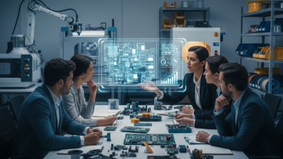
In the rapidly evolving landscape of electronics PCB manufacturing, efficiency and precision are paramount. According to the latest market report by Technavio, the global PCB market is expected to grow by nearly $20 billion between 2021 and 2025. This growth highlights the importance of robust manufacturing techniques. As Dr. Emily Chen, a leading expert in PCB technology, notes, "Innovation in PCB manufacturing techniques is crucial for meeting rising industry demands."
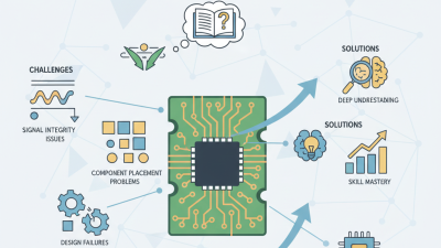
Modern electronics PCB manufacturing encompasses various techniques that enhance performance and reliability. The shift towards miniaturization and higher functionality necessitates continuous improvement. However, not all methods yield the same results. Some traditional techniques may fail to meet contemporary standards, highlighting areas for reevaluation and improvement.
Understanding these 10 best techniques can provide manufacturers with a competitive edge. They guide the way towards sustainable practices and efficient production. Yet, manufacturers must be willing to adapt and innovate. The challenge lies in balancing traditional proficiency with the need for new technologies. Progress in electronics PCB manufacturing requires a commitment to both quality and adaptability.
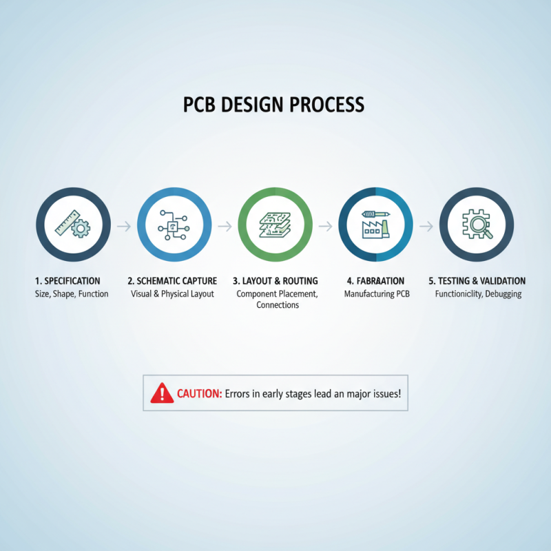
Understanding PCB manufacturing techniques is crucial for anyone in the electronics industry. The global PCB market is projected to reach $80 billion by 2026, according to industry reports. This growth reflects the demand for innovative manufacturing methods that continuously evolve. Techniques like subtractive, additive, and hybrid technologies are pivotal for optimizing production efficiency.
Subtractive manufacturing involves removing material to create circuit paths. It is widely used due to its cost-effectiveness and reliability. However, this method can result in more waste. On the other hand, additive manufacturing builds circuits layer by layer. It's a promising technique that minimizes waste but requires more advanced technology. Many companies struggle to integrate these techniques effectively, facing challenges with scalability and quality control.
Hybrid techniques combine the best of both worlds. These methods promise increased flexibility but come with their own unique challenges. The complexity of integrating different processes can lead to defects. Research indicates that up to 10% of PCBs produced can experience failures in the field. Continuous monitoring and refinement of manufacturing techniques are essential to address these issues. The right approach ensures high-quality PCBs that meet growing market demands.
In PCB fabrication, choosing the right materials is crucial. The most commonly used substrate is FR-4, which is a composite of fiberglass and epoxy resin. This material is favored for its excellent electrical insulation and thermal stability. Reports indicate that FR-4 accounts for approximately 90% of the global PCB market. However, its rigidity can lead to cracking under stress, prompting engineers to seek alternatives.
Another important material is polyimide. This polymer offers superior heat resistance and flexibility, making it ideal for high-performance applications. It can withstand temperatures over 200 degrees Celsius. It's crucial for flexible PCBs. However, it's also more expensive, and not every application justifies the increased costs.
Lastly, copper is widely used for conductive pathways on PCBs. Thin copper layers are essential for high-frequency devices. A report from an industry study suggests that copper-based materials dominate due to their conductivity but are also subject to oxidation. Engineers must address this issue during manufacturing to ensure long-term reliability. Balancing performance and cost remains a challenge in material selection.
The PCB design process involves several crucial steps. Each step demands careful attention to detail. Designers often start with defining specifications. This includes size, shape, and functionality. Creating schematic diagrams comes next. This part is visual and vital. Mistakes here can lead to significant issues later.
Once the schematic is in place, it's time for layout design. This is where the real magic happens. Components are arranged on the board. Connections are drawn to form electrical paths. Designers must consider spacing and signal integrity. Sometimes, they overlook these aspects. The result can be a poorly functioning PCB.
After layout, the next stage is design verification. This involves checking for errors. Designers often miss out on small mistakes. A simple oversight can lead to a failed prototype. Testing tools play a critical role in this phase. Many designers face challenges here. Lastly, once verified, the design is sent for manufacturing. However, even at this stage, there might be flaws that need revisiting.
PCB fabrication involves several methods with distinct applications. The most common techniques include etching, laminating, and screen printing. Etching is vital for creating precise circuit patterns. According to industry reports, about 70% of PCBs leverage this technique. It relies on removing excess copper to form traces. This method is cost-effective but can lead to inaccuracies without careful calibration.
Laminating creates multi-layered boards essential for compact electronics. This method enables the integration of complex circuits in smaller spaces. Research indicates that the demand for multilayer PCBs rose by 15% in recent years. However, balancing layer thickness and dielectric materials poses challenges. Screen printing, frequently used for applying solder masks, has become popular. It allows high-volume production but requires significant setup time.
While these methods are common, they come with their downsides. For instance, etching can produce waste materials, impacting environmental sustainability. Laminating can introduce internal defects during the press process. It's clear that while PCB fabrication methods continue to evolve, they still demand critical evaluation. A balance between efficiency and precision remains essential in this dynamic industry.
| Technique | Description | Applications |
|---|---|---|
| Etching | A process that removes unwanted copper from a PCB to form the required circuit pattern. | Consumer Electronics, Communication Devices |
| Laminating | A technique involving bonding multiple layers of PCB material to create multilayer boards. | High-Density Applications, Digital Devices |
| Drilling | Creating holes in the PCB for component leads and vias using precise drilling machines. | All Types of PCBs |
| Soldering | The process of joining components to the PCB using solder. | Assembly of Electronic Devices |
| Plating | Depositing a layer of metal on the PCB surface for better conductivity and protection. | RFID Tags, High-Frequency Circuits |
| Screen Printing | Applying conductive ink to the PCB to create printed circuits or to mark components. | Indication of Component Placement |
| V-Cutting | A technique for scoring a board to allow easy separation along designated lines. | Modular Circuits, Prototyping |
| Routing | Cutting away areas of the PCB substrate to create specific shapes and paths for the circuit. | Custom PCB Designs |
| Surface Mount Technology (SMT) | A method for mounting electronic components directly onto the surface of PCBs. | Compact Devices, Consumer Electronics |
| Hybrid PCB Technology | Integrating various technologies, including printed circuit boards and flexible circuits. | Wearable Technology, Medical Devices |
In today's rapidly changing electronics industry, advanced PCB production techniques are essential. These techniques enhance efficiency, reduce costs, and improve product quality. One of the notable methods is the use of multi-layer PCBs. These boards allow for more connections in a smaller space. Their compact design supports more complex electronic devices.
Another approach is automation in PCB manufacturing. Automated soldering processes minimize human error and speed up production. This can result in a higher yield of functional boards. However, automation requires significant upfront investment. Small manufacturers might find it challenging to adopt fully automated lines.
Flex PCBs have also emerged as a game-changer. These boards can bend and twist, opening new design possibilities. They are lighter and can fit into tighter spaces, making them ideal for mobile devices. But the flexibility comes with its own set of challenges. The manufacturing process is often more complex, requiring specialized equipment. Overall, while advanced techniques in PCB production bring significant benefits, they also require careful consideration of potential drawbacks and limitations.