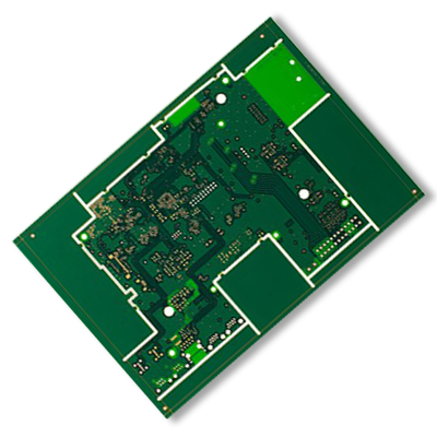
HDI (High Density Interconnect PCB)

HDI (High Density Interconnect PCB)

Multilayer boards with a higher connection pad density than standard boards, with finer lines/spaces, smaller via holes and capture pads allowing microvias to only penetrate select layers and also be placed in surface pads.

What is a HDI (High Density Interconnect PCB)?

High-Density Interconnect (HDI) Printed Circuit Boards represent a significant evolution in PCB technology. With the relentless advancement of electronic devices towards miniaturisation and enhanced functionality, HDI PCBs have become integral in modern electronics. They offer higher circuitry density than traditional PCBs, enabling more features in smaller form factors. This introduction aims to provide a foundational understanding of HDI PCBs, outlining their structure, manufacturing process, applications, advantages, challenges, and future trends in this technology.

HDI PCBs are a preferred choice for high-performance, space-constrained applications.
HDI Printed Circuit Boards are characterised by their densely packed electronic components and fine lines. Unlike conventional PCBs, HDI PCBs utilise microvias, which are tiny holes drilled by lasers, to connect the layers of the board. These microvias can be blind or buried, connecting only specific layers or wholly enclosed within the PCB.

The main difference between HDI and traditional PCBs lies in their layer structure and via technology. HDI PCBs have more layers and use microvia technology, allowing for a more compact design. This results in a smaller board size but more functionality packed in, compared to traditional PCBs with larger vias and fewer layers.

Other technical specifications

Feature Technical specification
Number of layers 4 - 22 layers standard, 30 layers advanced
Technology highlights Multilayer boards with a higher connection pad density than standard boards, with finer lines/spaces, smaller via holes and capture pads allowing microvias to only penetrate select layers and also be placed in surface pads.
HDI builds 1+N+1, 2+N+2, 3+N+3,4+N+4, any layer in R&D
Materials FR4 standard, FR4 high performance, Halogen free FR4, Rogers
Copper weights (finished) 18μm - 70μm
Minimum track and gap 0.075mm / 0.075mm
PCB thickness 0.40mm - 3.20mm
Maximum dimensions 610mm x 450mm; dependent upon laser drilling machine
Surface finishes available OSP, ENIG, Immersion tin, Immersion silver, Gold fingers
Minimum mechanical drill 0.15mm
Minimum laser drill 0.10mm standard, 0.075mm advanced
Heading #1
Heading #2
Heading #3
Simple content
Simple content
Simple content

Search our website