How to Design a PCB Circuit Board for Electronics Projects?
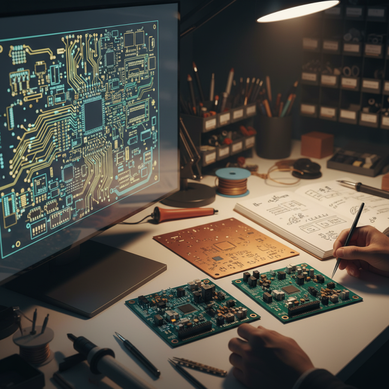
Designing a PCB circuit board for electronics projects can be both exciting and challenging. A well-designed circuit board is crucial for the performance and reliability of any electronic device. It serves as the backbone that connects all components, ensuring they work harmoniously.
However, the design process is not always straightforward. Many beginners struggle with layout and component placement. Mistakes can lead to signal interference or circuit failures. It’s essential to choose the right materials and tools for your PCB circuit board. Investing time in understanding design software can significantly improve your results.
Creating a PCB circuit board requires careful thinking and creativity. Skipping important steps can result in flawed designs. Reflecting on past mistakes can lead to better outcomes in future projects. Every successful design begins with a solid concept and attention to detail.
Understanding the Basics of PCB Circuit Board Design
Designing a PCB circuit board is an essential skill for projects in electronics. A basic understanding of PCB design begins with learning about circuit layouts. You should familiarize yourself with schematic design software. This allows for a visual representation of your circuit before fabrication. Ensure each component is correctly placed and connected. Mistakes often happen, leading to failures in the final product.
When laying out your PCB, think about the size and shape. Compact designs can save space, but they complicate assembly. Leave enough room for heat dissipation and signal integrity. Routing traces can be tricky. Keep them as short as possible to avoid interference. Sometimes, you may find that your traces are too close, risking short circuits.
Tips: Always double-check connections. Use a simple checklist to minimize errors. For beginners, starting with a single-layer board can be helpful. As you grow more confident, explore multiple layers for more complex projects. Mistakes are part of the learning journey, so reflect on each project. Analyze what works and what doesn’t, adjusting your approach for future designs. This iterative process will improve your skills over time.
How to Design a PCB Circuit Board for Electronics Projects? - Understanding the Basics of PCB Circuit Board Design
| Component |
Function |
Material Used |
Layer Count |
Typical Thickness (mm) |
| Resistor |
Limits current flow |
Carbon film / Metal film |
1-2 |
0.5 - 2.0 |
| Capacitor |
Stores electrical energy |
Ceramic / Electrolytic |
1-4 |
0.5 - 2.5 |
| Inductor |
Stores energy in a magnetic field |
Copper wire / Ferrite core |
1-2 |
0.5 - 3.0 |
| Transistor |
Amplifies or switches electronic signals |
Silicon |
1-3 |
0.5 - 1.5 |
| Microcontroller |
Controls devices and processes data |
Silicon |
1-6 |
1.0 - 3.0 |
Choosing the Right Materials for Your PCB Project
When designing a PCB, choosing the right materials is crucial for your project. The substrate is vital. You can select from various materials like FR-4 or polyimide. FR-4 is common and affordable. It offers good thermal resistance. Polyimide handles higher temperatures but is pricier.
Consider the copper thickness as well. For most projects, 1 oz per square foot is standard. Thicker copper can handle higher currents but can affect flexibility. Be cautious about your layout. Complex designs can create issues. The wrong material choice may lead to failures during testing.
Tips: Always prototype with cheaper materials first. This will save costs and allow quick revisions. Test different thicknesses to see what works best. Measure for thermal conductivity too. This can prevent overheating. Learning about material characteristics is essential. Mistakes in material selection can lead to wasted time and resources.
Step-by-Step PCB Design Process: From Schematic to Layout
Designing a PCB circuit board begins with a solid schematic. This is your blueprint. It showcases how all components connect. Each element, from resistors to capacitors, should be clearly labeled. Using software simplifies this process. Ensure that every connection is precise. Errors in this stage can lead to faults later.
Transitioning to layout requires attention to detail. Place components thoughtfully to minimize space while avoiding clutter. Keep high-frequency parts away from others. This prevents interference. Routing traces can be tricky. It’s crucial to maintain proper width and spacing. Incorrectly sized traces can overheat. While it’s easy to rush, take time to reassess your layout.
Layout iterations are often necessary. Expect to revisit your design multiple times. Seek feedback from peers to gain fresh perspectives. Sometimes, what seems fine to you may have flaws. Remember, mistakes in PCB design can be costly. Continuous learning from these experiences is essential for improvement in future projects.
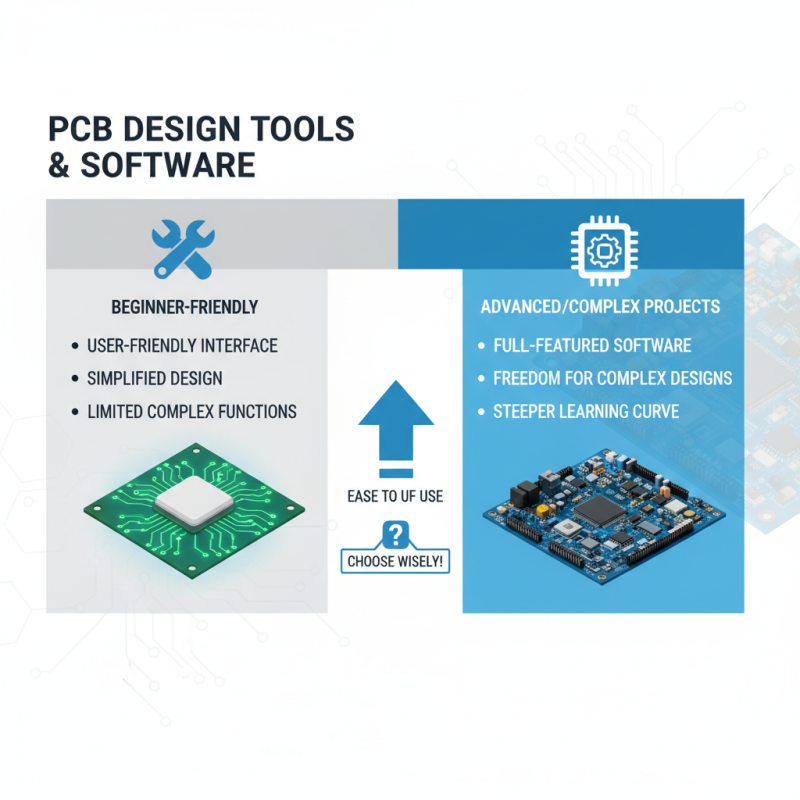
Tools and Software for Designing PCB Circuit Boards
When designing PCB circuit boards, choosing the right tools and software is crucial. Various options are available depending on your skill level and project complexity. Beginners may find user-friendly tools helpful. Intuitive interfaces can simplify the design process significantly. However, these tools can restrict complex functions.
For those with more experience, advanced software may be necessary. These programs often offer powerful features, including 3D visualization and design rule checks. Yet, the learning curve can be steep. Mastery might take time and practice. It's essential to explore the available resources and tutorials.
Simulation tools are also vital. They help in testing designs before creating physical prototypes. Errors can be costly and time-consuming. Many tools provide real-time feedback on electrical performance. However, relying too much on simulations might lead to oversight. Understanding components in the physical realm is still essential for successful designs. Balancing software capabilities with foundational knowledge is key.
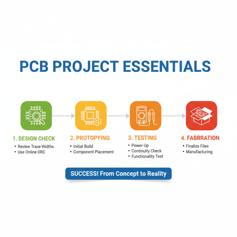
Testing and Fabricating Your PCB for Electronics Projects
Testing and fabricating your PCB is crucial for a successful electronics project. After designing your circuit, prototyping is the next logical step. Start by checking your design files meticulously. Errors like incorrect trace widths can lead to performance issues. Use an online PCB checker to catch common mistakes.
Once your design is verified, it's time to fabricate your PCB. Choose a suitable PCB manufacturer, considering factors like cost and turnaround time. Many offer online tools for placing orders. Providing clear specifications is vital. Double-check your design rules before submitting files. It’s common to overlook details such as layer stacking or drill sizes.
After fabrication, perform rigorous testing. If the board does not work, analyze it carefully. Look for short circuits or soldering issues. Use a multimeter to test connections. Sometimes, the problem lies in the design or components rather than the board itself. Reflection on these points can lead to better designs in the future.