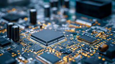
10 Essential Tips for Successful PCB Assembly Every Engineer Should Know
In the fast-evolving world of electronics, the importance of efficient and reliable PCB assembly cannot be overstated. As a key process in the manufacturing of electronic devices, PCB assembly serves as the backbone for functionality and performance. Engineers must navigate a myriad of challenges, from design intricacies to quality assurance, making it essential to arm oneself with knowledge and best practices in this field. This article presents ten essential tips for successful PCB assembly that every engineer should know, ensuring that the backbone of their electronic products is robust and effective.

Understanding the complexities involved in PCB assembly is crucial for achieving optimal performance and minimizing costly errors. Whether you are a seasoned engineer or just starting in the industry, these insights will guide you through the pivotal aspects of the assembly process. From selecting the right materials to ensuring precise soldering techniques, the following tips will help streamline PCB assembly, enhance product reliability, and ultimately elevate your engineering projects. Join us as we delve into these indispensable strategies that promise to refine your PCB assembly process and equip you with the tools necessary for success in today's competitive landscape.
Key Factors Influencing PCB Assembly Yield and Quality Metrics
When it comes to PCB assembly, several key factors significantly influence the yield and quality metrics of the final product. One of the most critical elements is the selection of materials. High-quality substrates and solder paste can drastically impact the durability and performance of the PCBs. Engineers must ensure compatibility among components and materials to minimize defects, such as shorts and open circuits, that arise from using subpar or mismatched materials.
Another important factor is the accuracy of the assembly process itself. Precision in placement is vital; even a slight misalignment can lead to functionality issues. Utilizing advanced assembly equipment and automation can enhance positioning accuracy and reduce human error. Additionally, meticulous attention to the soldering process, ensuring that temperatures and timings are optimal, is crucial to achieving reliable joints and improving overall yield. Regular monitoring and feedback during production can also help identify and rectify potential problems quickly, leading to higher quality outcomes and increased efficiency in PCB assembly.

Importance of Material Selection: Sourcing High-Quality Components
The importance of material selection in PCB assembly cannot be overstated. Sourcing
high-quality components is a critical step in the engineering process, as it directly affects the performance, reliability, and longevity of the final product.
Engineers must pay close attention to the specifications of the materials they choose, ensuring they meet both industry standards and their project requirements. This includes understanding the
electrical properties, thermal characteristics, and mechanical behavior of components. Using inferior quality materials can lead to failures, increased costs,
and time delays, which can be detrimental in a competitive market.
Moreover, the selection of components should also align with the intended application of the PCB. For instance, components designed for
high-frequency environments might require different materials than those used in basic consumer electronics.
Engineers should collaborate closely with suppliers to ensure they are receiving materials that not only meet technical specifications but also come from
reputable sources. This partnership can enhance the overall quality of the PCB assembly process, ultimately leading to
innovative designs and successful product launches. Emphasizing
high-quality sourcing during the material selection phase is thus imperative for achieving optimal results in PCB assemblies.
Understanding the Role of Design for Manufacturability (DFM)
Design for Manufacturability (DFM) plays a crucial role in the success of PCB assembly. It involves designing electronic components and their layouts in a way that optimizes the manufacturing process, reducing complexity and potential errors. By incorporating DFM principles early in the design phase, engineers can ensure that the PCB can be efficiently produced, assembled, and tested. This not only minimizes production costs but also enhances product reliability, as designs that are easier to manufacture tend to have fewer issues in the field.
Additionally, engineers should consider factors such as component placement, pad sizes, and solder mask design while applying DFM guidelines. Strategically placed components can facilitate easier assembly and improve the overall robustness of the PCB. Moreover, selecting readily available components can prevent delays in the manufacturing process caused by sourcing difficulties. Emphasizing DFM not only streamlines production but also fosters better communication between design and manufacturing teams, leading to more cohesive workflows and ultimately a higher quality end product.
10 Essential Tips for Successful PCB Assembly
This bar chart represents the effectiveness of various tips for successful PCB assembly as rated by engineers. Each tip is scored on a scale of 1 to 10, indicating its significance in the assembly process. Understanding these tips can greatly enhance the efficiency and quality of PCB assembly projects.
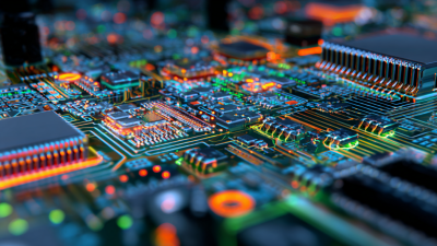
Common PCB Assembly Techniques: Soldering, Surface Mount, and Through-Hole
When it comes to PCB assembly, understanding the common techniques is crucial for engineers looking to ensure efficient and reliable production. Soldering remains one of the most fundamental methods, allowing for secure connections between components and the PCB. Various soldering techniques, including hand soldering and reflow soldering, cater to different assembly needs.
Hand soldering is often employed for prototyping or repairs, while reflow soldering is widely used in mass production due to its ability to apply heat uniformly, ensuring consistent solder joints.
In addition to soldering, surface mount technology (SMT) and through-hole technology (THT) play pivotal roles in modern PCB assembly. SMT involves placing components directly onto the surface of the PCB, which allows for higher component density and reduced size, making it ideal for compact designs.
On the other hand, THT involves inserting components into pre-drilled holes on the PCB and is traditionally used for larger components or those requiring higher durability. Each technique has its own set of advantages and applications, and understanding their differences is essential for engineers to choose the right one for their specific project requirements.
Utilizing Advanced Testing Methods to Ensure PCB Reliability
When it comes to ensuring the reliability of printed circuit boards (PCBs), advanced testing methods play a pivotal role. Engineers must implement these techniques at various stages of the PCB assembly process to identify potential issues before they escalate into significant failures. Techniques such as Automated Optical Inspection (AOI) allow for the detection of solder joint defects and misplaced components, significantly enhancing the overall quality control. By integrating AOI into the assembly line, engineers can quickly pinpoint flaws, ensuring that only the highest quality boards proceed to the next phase.
Another critical method is functional testing, where complete assemblies are subjected to real-world conditions to verify their operational efficacy. This testing simulates the actual environments in which the PCB will function, allowing engineers to observe performance under stress. Additionally, employing thermal imaging can reveal hotspots that indicate potential failure points due to excessive heat. Combining these advanced testing methodologies not only streamlines the assembly process but also fosters the production of robust and reliable PCBs that meet industry standards and customer expectations.