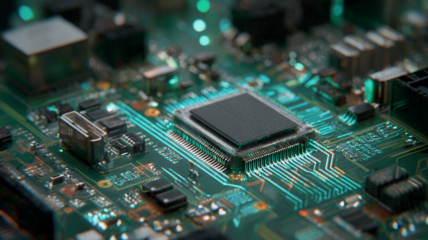
Exploring the Future of PCB Assembly: Innovations That Could Revolutionize Electronics
The landscape of electronics manufacturing is on the brink of a significant transformation, propelled by groundbreaking innovations in PCB assembly. As the demand for faster, more efficient, and environmentally friendly production methods continues to rise, the future of this critical process is being redefined. This article will explore the latest advancements in PCB assembly techniques, highlighting how emerging technologies like automation, artificial intelligence, and novel materials are set to revolutionize the industry.
We will delve into how these innovations not only enhance product quality and reduce lead times but also contribute to sustainable manufacturing practices. Join us as we navigate the exciting possibilities that lie ahead for PCB assembly and the broader implications for the electronics sector as a whole.
Future Materials in PCB Assembly: The Shift Towards Eco-Friendly Options
The future of PCB assembly is increasingly leaning towards eco-friendly materials that promise not only to reduce the environmental footprint but also to enhance the efficiency of electronic devices. As manufacturers seek sustainable solutions, biodegradable substrates and lead-free soldering materials are gaining traction. These innovations support the industry's goal of minimizing waste and energy consumption, paving the way for a greener electronics landscape.
Tip: When considering eco-friendly options, look for suppliers who prioritize sustainable practices and can provide certifications for their materials. This ensures that your PCB assembly process aligns with environmental standards.
In addition to sustainability, advancements in materials science are introducing flexible and lightweight alternatives that can drastically change the design and functionality of PCBs. These new materials enable more intricate designs while maintaining durability, thereby elevating the performance of devices ranging from smartphones to wearable tech.
Tip: Keep an eye on emerging trends in materials science to stay ahead of the curve. Experimenting with innovative materials can significantly enhance your product's market competitiveness and appeal to environmentally conscious consumers.
Automation Trends: How Robotics Are Redefining PCB Manufacturing Process
The landscape of PCB manufacturing is undergoing a significant transformation, largely driven by advancements in automation and robotics. As the demand for more complex and compact electronic devices continues to rise, traditional manual assembly methods struggle to keep pace. Automated solutions are emerging as a game-changer, allowing manufacturers to enhance precision, reduce labor costs, and increase production speeds. Robots equipped with advanced vision systems can now accurately place and solder components on PCBs, minimizing human error and enhancing overall quality.
Furthermore, the integration of AI and machine learning into robotic systems is pushing the envelope even further. These technologies enable predictive maintenance and real-time monitoring of assembly lines, ensuring that production processes remain efficient and downtime is minimized. The synergy between robotics and automation not only streamlines the PCB manufacturing process but also opens up new opportunities for customization and flexibility in production. As companies adopt these innovative solutions, the future of PCB assembly looks promising, paving the way for smarter and more sophisticated electronics.
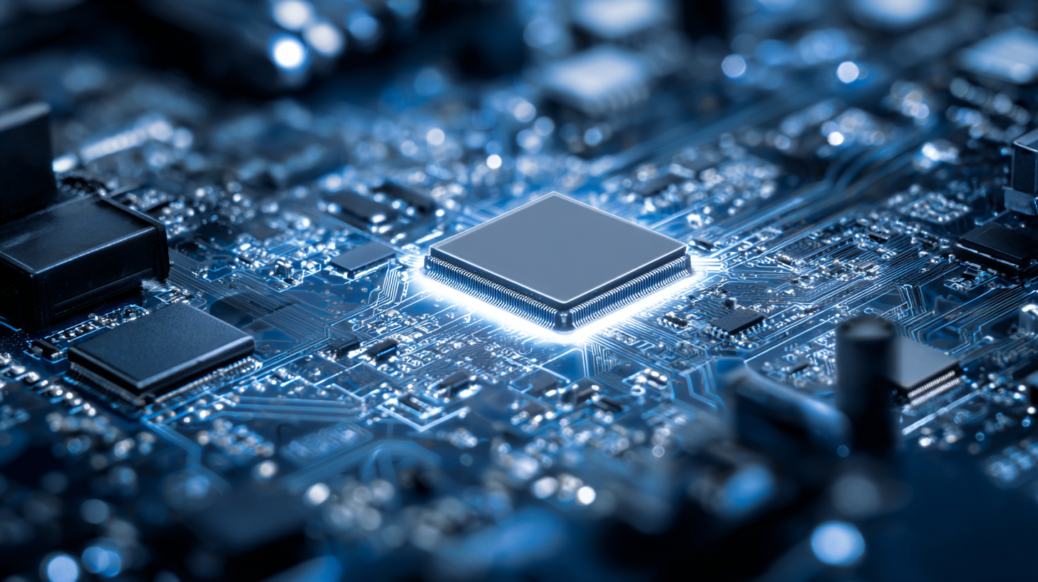
Exploring Innovations in PCB Assembly
Advanced Design Software: Streamlining PCB Layout and Prototyping
The advent of advanced design software has transformed the landscape of PCB layout and prototyping, paving the way for significant innovations in electronics manufacturing. According to a report by MarketsandMarkets, the PCB design software market is poised to grow from $2.41 billion in 2021 to $3.63 billion by 2026, reflecting a compound annual growth rate (CAGR) of 8.5%. This advancement not only enhances the efficiency of design processes but also significantly reduces production time and costs.
One of the key features of modern PCB design tools is their ability to integrate artificial intelligence (AI) and machine learning algorithms, allowing designers to automate complex tasks and optimize layouts for performance and manufacturability. A study from the Electronics Design Automation Consortium indicates that integrating AI-driven software into PCB design can reduce time-to-market by as much as 50%. Furthermore, these advanced tools provide real-time simulations and error-checking capabilities, greatly minimizing the risks of design flaws and ensuring greater reliability in electronic applications. As the demand for intricate and compact circuit boards continues to rise, leveraging sophisticated design software is essential for staying competitive in the fast-evolving electronics industry.
Exploring the Future of PCB Assembly: Innovations That Could Revolutionize Electronics
| Innovation |
Description |
Benefits |
Impact on PCB Assembly |
| Advanced Design Software |
Software tools that enhance layout design and reduce prototyping time. |
Improves accuracy, saves time and reduces costs. |
Facilitates faster iterations and more complex designs. |
| AI-Driven Design Tools |
Artificial intelligence assists in optimal layout and routing. |
Enhanced efficiency and reduced human error. |
Accelerates the design process significantly. |
| 3D PCB Printing |
Utilizing 3D printing for rapid PCB prototyping. |
Allows for complex geometries and faster turnarounds. |
Greater flexibility in design experimentation. |
| Cloud-Based Collaboration Tools |
Platforms for real-time design collaboration. |
Fosters teamwork and streamlines communication. |
Reduces design bottlenecks and improves project timelines. |
| Automated Testing Solutions |
Techniques that automate the testing of PCB functionality. |
Increases reliability and reduces time spent on debugging. |
Ensures high-quality production standards. |
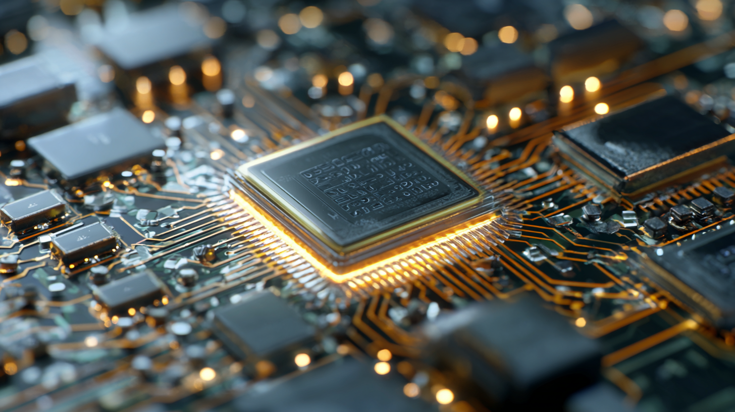
3D Printing in PCB Assembly: A Game Changer for Custom Designs
The integration of 3D printing technology into PCB assembly is poised to transform the landscape of electronics, offering unprecedented benefits for custom designs. This innovative approach allows engineers to prototype intricate circuit layouts with a level of precision and complexity that traditional methods simply cannot achieve. By fabricating components layer by layer, manufacturers can reduce production lead times, minimize costs, and respond swiftly to market demands, making expedited iterations much more feasible.
Tip: When considering 3D printing for PCB assembly, start with a clear design plan. Leverage software tools that allow for easy modifications and optimizations, which can significantly enhance the efficiency of the printing process.
Moreover, 3D printing facilitates the development of personalized electronics, allowing for tailored solutions to meet unique consumer needs. This flexibility encourages creativity, enabling designers to explore unconventional geometries and functionalities that are often limited by conventional manufacturing methods. The ability to quickly adapt designs can lead to breakthroughs in sectors like wearable technology and IoT devices, where customization is key.
Tip: Collaborate with 3D printing specialists who understand both PCB design and manufacturing processes. Their expertise can help streamline production and ensure high-quality results that align with your innovative vision.
Innovative Testing Technologies: Ensuring Quality and Reliability in Production
As the electronics industry continues to evolve, innovative testing technologies are becoming paramount in ensuring quality and reliability in PCB assembly. These advancements not only enhance the efficiency of testing processes but also significantly reduce the likelihood of defects in the final product. Automated optical inspection (AOI) systems are now equipped with artificial intelligence, enabling them to learn from previous inspections and improve their detection capabilities. This allows for a more accurate assessment of solder joints, component placements, and overall board integrity, ultimately leading to higher-quality electronics.
Moreover, the integration of advanced data analytics tools into the testing process facilitates real-time monitoring and predictive maintenance. By analyzing the data collected during production, manufacturers can identify potential issues before they escalate. This proactive approach greatly minimizes downtime and production costs, enhancing the overall reliability of electronic components. Furthermore, the use of X-ray inspection technology enables manufacturers to visualize internal structures of PCB assemblies, providing deeper insights into potential defects that traditional testing methods might miss. Together, these innovative testing technologies are set to redefine quality assurance standards in electronics manufacturing.