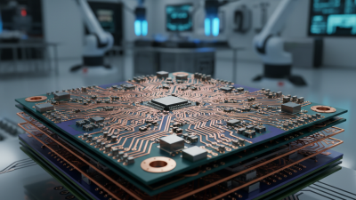
Why Choose Multilayer PCB for Your Next Electronics Project
In the rapidly evolving world of electronics, the choice of printed circuit board (PCB) technology plays a crucial role in the success of any project. Among various options, multilayer PCBs have emerged as a preferred solution due to their ability to support high-density interconnections and compact designs. According to a recent market analysis by Research and Markets, the global multilayer PCB market is projected to reach $12.5 billion by 2027, highlighting the growing demand for advanced electronic applications in sectors such as telecommunications, automotive, and medical devices.
Industry expert Dr. Emily Chen, a leading authority in PCB technology, emphasizes the significance of multilayer designs in modern electronics: "Multilayer PCBs not only enhance functionality by allowing more complex and compact routing but also improve signal integrity and reduce electromagnetic interference." This perspective underscores the innovative edge that multilayer PCBs provide, making them indispensable for engineers aiming to deliver cutting-edge electronic solutions.
As projects become increasingly sophisticated, the technical advantages of multilayer PCBs—such as space-saving capabilities, improved electrical performance, and enhanced thermal management—become vital considerations. In optimizing performance and reliability, multilayer PCBs stand out as a pivotal choice for designers looking to push the boundaries of what is possible in their next electronics project.

Understanding Multilayer PCBs: Definition and Structure
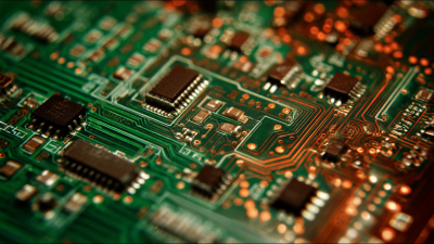
Multilayer printed circuit boards (PCBs) are a vital component in the modern electronics landscape, distinguished by their complex structure composed of multiple layers. Typically, they consist of three or more conductive layers, which are interleaved with insulating materials. This multi-layer configuration allows for a significant increase in the density of circuitry, accommodating more components in a compact space while maintaining performance. By efficiently utilizing vertical space, multilayer PCBs help designers achieve intricate circuit layouts that would be impossible with single or double-sided PCBs.
The structure of a multilayer PCB includes core layers and prepreg layers, which are bonded together under heat and pressure. The core layers are made of a rigid dielectric material, often FR-4, that provides structural support and electrical insulation. Prepregs, which are sheets of woven glass fiber pre-impregnated with resin, act as insulating layers. These layers are strategically placed to create a layered assembly that facilitates complex interconnections while minimizing electromagnetic interference. This makes multilayer PCBs an excellent choice for high-frequency applications and multi-functional devices, where performance and reliability are critical. The intricate design possibilities inherent in multilayer PCBs enable the creation of sophisticated electronics that meet evolving consumer and industrial demands.
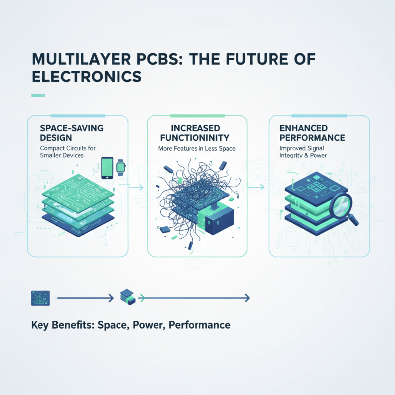
Advantages of Multilayer PCBs in Electronics Projects
Key Advantages of Using Multilayer PCBs in Electronics Projects
Multilayer PCBs have become increasingly popular in modern electronics projects due to their numerous advantages. One of the key benefits is the ability to save space without compromising functionality. With multiple layers stacked together, engineers can design compact circuits that fit into smaller enclosures, making them ideal for devices with limited space, such as smartphones and wearables. This space-saving aspect also facilitates the integration of more complex functionalities without increasing the overall size of the device.
Another significant advantage of multilayer PCBs is their enhanced signal integrity and reduced electromagnetic interference. By providing better electrical performance through controlled impedance and reduced crosstalk, multilayer designs help maintain signal quality, which is crucial for high-speed applications. This characteristic is particularly beneficial in fields such as telecommunications and computing, where reliable data transmission is essential. Additionally, the construction of multilayer PCBs allows for greater routing flexibility, enabling intricate designs that can accommodate various components and connections efficiently.
Design Considerations When Choosing Multilayer PCBs
When selecting a multilayer PCB for your electronics project, several design considerations must be prioritized to ensure optimal performance and functionality. First, the layer count is crucial; it not only affects the complexity and size of the board but also its ability to handle high-speed signals and dense circuitry. More layers can facilitate better signal integrity and minimize electromagnetic interference, making them suitable for advanced applications such as RF and high-speed digital devices.
Another important aspect to consider is the material selection. Different laminates and substrates offer varying thermal and electrical properties, impacting the reliability and efficiency of the PCB. For projects that require high thermal conductivity or specific dielectric properties, choosing the right material is essential. Additionally, the stack-up design should be thoughtfully planned to balance impedance control and minimize crosstalk between layers. Overall, careful consideration of these factors when opting for a multilayer PCB can lead to enhanced performance and a more robust final product.
Applications and Industries That Benefit from Multilayer PCBs
Multilayer PCBs (Printed Circuit Boards) have become essential in various applications across multiple industries due to their
compact design and enhanced performance capabilities. One notable application is in telecommunications, where
high-frequency signals and complex routing are critical. The use of multilayer PCBs allows for multiple layers to
interconnect various components efficiently, ensuring better signal integrity and reduced electromagnetic interference.
This is particularly important in devices such as smartphones and
routers that require reliable performance for data transmission.
Another industry that significantly benefits from multilayer PCBs is the medical sector.
Medical devices often require advanced functionalities and miniaturization, which multilayer PCBs can provide. Devices such as
MRI machines and portable monitoring equipment utilize multilayer technology to house sophisticated circuits within a limited space while maintaining operational reliability.
By accommodating intricate designs, multilayer PCBs facilitate innovation in medical technology, leading to better patient outcomes and more effective treatments.
Cost Implications of Multilayer PCB Manufacturing and Design
When considering the cost implications of multilayer PCB manufacturing and design, it's essential to recognize that while the initial investment may be higher compared to single-layer or double-layer options, the long-term benefits often outweigh these upfront costs. According to a report from the IPC (Association Connecting Electronics Industries), multilayer PCBs can reduce the overall size of electronic devices, effectively allowing for more compact designs. This not only decreases material costs for enclosures but also minimizes the logistics expenses associated with transporting larger or multiple boards.
Additionally, multilayer PCBs can enhance performance features such as signal integrity and power distribution, which can lead to improved reliability. Data from Research and Markets indicates that the global multilayer PCB market is projected to reach approximately $10 billion by 2025, driven primarily by growing demands in sectors like automotive, telecommunications, and consumer electronics. The increased complexity and higher layer count do require more sophisticated manufacturing processes, but as the technology continues to evolve, manufacturers are finding more cost-effective methods that offset these expenditures. Investing in multilayer technology can ultimately contribute to a more robust and efficient product lifecycle, making it a strategic choice for engineers and designers in today's competitive market.