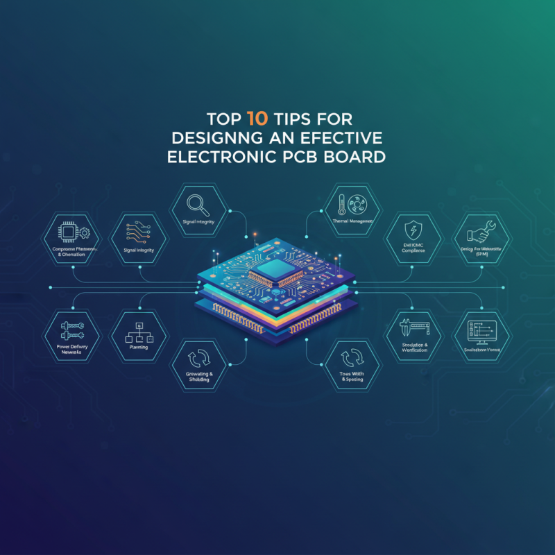
Top 10 Tips for Designing an Effective Electronic PCB Board
In the rapidly evolving field of electronics, the design of an electronic PCB board is a critical cornerstone that can determine the success or failure of a device. Leading experts in the industry emphasize the importance of thoughtful design strategies. For instance, Dr. Emily Carter, a renowned PCB design engineer at Tech Innovations, states, “An effective electronic PCB board not only optimizes performance but also significantly reduces manufacturing costs and time.” This insight highlights the necessity for a comprehensive approach to PCB design, where every decision can have far-reaching implications.
Designing an electronic PCB board involves a complex interplay of technical skills and creative problem-solving. With advancements in technology and increasing demands for efficiency, engineers must be equipped with the latest knowledge and skills to create boards that meet contemporary requirements. By following best practices and leveraging innovative design tools, they can craft PCB layouts that maximize functionality while adhering to tight timelines and budgets. This article presents the top ten tips for designing an effective electronic PCB board, aimed at helping professionals navigate the intricacies of PCB design and enhance their projects' success.
Understanding the Basics of Electronic PCB Design Principles
When embarking on the journey of electronic PCB design, understanding the foundational principles is crucial for achieving an effective outcome. At the core of PCB design lies the concept of a circuit’s functionality and layout. A well-designed PCB not only serves to connect various electronic components but also ensures optimal signal integrity and minimizes interference. Key principles include understanding the role of trace width and spacing, which are essential for handling current and preventing signal degradation. Additionally, incorporating a solid ground plane can significantly improve the overall stability of the circuit.
Another fundamental aspect of PCB design is the selection and arrangement of components. Careful consideration must be given to the placement of parts in order to streamline the manufacturing process and enhance performance. Components should be positioned with adequate spacing to facilitate heat dissipation and allow for easy access during soldering. Moreover, designers should prioritize the use of design rules checking (DRC) tools to catch potential errors early in the design process. By adhering to these principles, designers can create PCBs that are not only functional but also efficient and reliable.
Key Considerations for Selecting PCB Materials and Components
When selecting PCB materials and components, it is essential to consider the specific requirements of your electronic design. The type of base material largely influences the board's thermal and mechanical properties, electrical performance, and overall reliability. For instance, FR-4 is a commonly used dielectric material that balances affordability and good electrical performance for many applications. However, for high-frequency or high-temperature environments, materials such as PTFE or polyimide may be more suitable due to their superior thermal stability and low dielectric loss.
Another critical aspect is the choice of components, which should align with the board's intended function and operational conditions. Factors such as the size, power rating, and mounting style of components should be matched with the PCB layout to ensure effective signal integrity and heat dissipation. Additionally, the environmental considerations, including moisture and chemical exposure, can dictate the need for protective coatings and conformal finishes that enhance longevity and durability. By addressing these key considerations early in the design process, you can significantly improve the performance and reliability of your electronic PCB boards.
Best Practices for Circuit Layout and Traces in PCB Design
When designing an electronic PCB, one of the most critical factors to consider is the layout of the circuit and the traces that connect various components. Effective circuit layout begins with strategically placing components to minimize the trace lengths between them, which reduces latency and decreases the potential for electromagnetic interference (EMI). Careful planning around the placement of sensitive components, such as oscillators and RF units, is essential to maintain signal integrity. Utilizing ground planes and proper decoupling capacitors can further enhance performance by providing stable voltage levels and reducing high-frequency noise.
Additionally, the design of traces plays a significant role in ensuring that the PCB functions efficiently. Designers should pay attention to the width of the traces to handle the expected current without overheating. Implementing differential pairs for high-speed signals is also crucial, as it allows the signals to be transmitted with greater immunity to noise. Furthermore, ensuring the correct spacing between traces helps to prevent crosstalk and interference. By adhering to these best practices in circuit layout and trace design, engineers can create PCBs that not only meet performance requirements but also enhance overall reliability and longevity.
Top 10 Tips for Designing an Effective Electronic PCB Board
This bar chart represents the importance of various best practices in PCB design based on a qualitative assessment from industry professionals. Each tip is rated on a scale of 1 to 10, with 10 being the most critical for effective PCB design.
Techniques for Effective Thermal Management in PCBs
Effective thermal management is crucial in PCB design, as it ensures the reliability and functionality of electronic devices. One key technique is the use of thermal vias, which facilitate heat dissipation from hot components to the layered internal structure of the PCB. By strategically placing thermal vias near heat-generating components, designers can enhance the heat transfer pathways and reduce localized heating, preventing thermal damage and improving overall performance.
Another important aspect of thermal management is the selection of materials with high thermal conductivity. Utilizing materials such as copper for traces and pads can improve heat dissipation significantly compared to standard PCB materials. Additionally, integrating heat sinks and thermal pads can further enhance the cooling of critical components by providing larger surfaces for heat exchange. Ensuring that components are well-spaced and have adequate airflow around them also contributes to better thermal performance, allowing for a more effective distribution of heat and minimizing potential hotspots on the board. By implementing these techniques, PCB designers can achieve a more balanced thermal profile, ensuring the longevity and reliability of the electronic devices.
Top 10 Tips for Designing an Effective Electronic PCB Board - Techniques for Effective Thermal Management in PCBs
| Tip Number |
Tip Description |
Advantages |
| 1 |
Use Thermal Vias |
Improves heat dissipation to inner layers. |
| 2 |
Incorporate Heat Sinks |
Enhances cooling for hot components. |
| 3 |
Select Appropriate Materials |
Affects thermal conductivity and performance. |
| 4 |
Optimize Component Placement |
Reduces heat buildup by spacing heat-generating parts. |
| 5 |
Utilize Copper Pour |
Acts as a thermal reservoir to spread heat. |
| 6 |
Implement Airflow Management |
Enhances thermal efficiency through ventilation. |
| 7 |
Monitor Temperature with Sensors |
Allows for real-time thermal management adjustments. |
| 8 |
Choose Power Supply Wisely |
Minimizes excessive heat from inefficient sources. |
| 9 |
Design for Future Upgrades |
Facilitates easier thermal enhancements later. |
| 10 |
Test and Iterate |
Ensures effective thermal performance through prototyping. |
Tips for Testing and Validating Your PCB Before Production
Testing and validating your PCB before production is a critical step in the design process, ensuring that the final product meets performance and reliability standards. Firstly, conducting comprehensive simulations can reveal potential design flaws early in the development cycle. Using software tools to simulate electrical signals and thermal performance allows designers to assess functionality under various conditions. This proactive approach can mitigate costly revisions later on, saving time and resources.
In addition to simulations, physical prototypes should be developed for real-world testing. Building a small batch of prototypes enables engineers to examine signal integrity, power distribution, and thermal management. Implementing rigorous testing protocols, such as functional and environmental tests, allows for verification of the PCB’s performance against specified requirements. Documenting these tests meticulously creates a valuable reference for future iterations and helps ensure that the final production units perform as intended. By prioritizing thorough testing and validation, designers can significantly enhance the reliability and success of their electronic PCBs in the market.