How to Understand the PCB Process for Beginners?
Understanding the PCB process can seem daunting for beginners. John Smith, a renowned PCB industry expert, states, "The PCB process is an art and a science." This highlights both the technical and creative elements involved in creating printed circuit boards.
The PCB process includes design, fabrication, and assembly. Each step requires careful attention to detail. For novices, it might feel overwhelming. Errors in design can lead to costly mistakes. Yet, learning from these challenges is part of the journey. Proper training and resources are crucial for mastering this process.
Mistakes often inspire growth. A beginner may struggle with intricate designs or selecting materials. These challenges encourage exploration. It’s essential to embrace trial and error. Each step in the PCB process brings you closer to expertise.
Understanding the Basics of PCB Design and Manufacturing
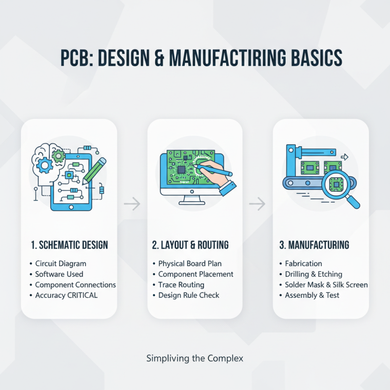
Understanding PCB design and manufacturing can seem daunting for beginners. At its core, a printed circuit board (PCB) is essential for connecting electronic components. The journey begins with schematic design. A designer uses software to create a diagram of the circuit. This diagram outlines how components connect. It’s important to ensure accuracy here, as even a small error can lead to significant problems later.
After schematic design, translating the diagram into a physical board begins. This stage is known as layout design. Designers arrange components and routes on the board. It can be tricky to balance size and functionality. Many beginners struggle with optimizing space, sometimes overlooking thermal issues or signal integrity. It's easy to forget that the board needs to fit into a larger system. Regularly revisiting design choices during this phase can save time and money.
Manufacturing follows the design phase. The PCB is fabricated based on the layout. While this may seem straightforward, various challenges can arise. Quality control is crucial, but it's often neglected. Poor quality can lead to failures in the final product, which is a costly mistake. It's advisable to learn from these mishaps. A commitment to understanding both design and manufacturing enhances the overall process and minimizes future errors.
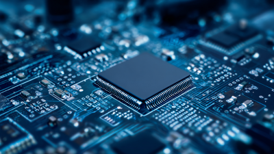
Key Components Involved in the PCB Process
Understanding the PCB process involves several key components. The first component is the design stage. In this phase, engineers create layouts using specialized software. They must ensure the blueprint meets specifications. Often, errors occur during this stage, leading to redesigns. These setbacks can impact timelines.
The next significant component is the fabrication process. Here, raw materials like copper and glass are transformed into printed circuit boards. This process requires precision and attention to detail. Any mistake in layering could result in faulty electronics. Factories often run tests, yet issues can still slip through.
Finally, the assembly stage takes place. Components like resistors and capacitors are placed on the boards. This stage is crucial, as the configuration affects performance. Misplacement can lead to circuit failures. Sometimes, teams rush to meet deadlines, leading to overlooked details. Reflection on these steps can enhance quality control in future projects.
Step-by-Step Guide to PCB Layout Design
Understanding the PCB layout design is crucial for beginners in electronics. The layout is the foundation of a successful PCB. Each component must be placed thoughtfully. According to industry reports, over 70% of PCB issues stem from layout errors. This highlights the importance of mastering this skill.
When creating a PCB layout, start with a schematic. This step ensures the circuit's functions are well-defined. After that, you can begin placing components. Choose positions that minimize long traces. Keep power and ground planes in mind. Good layout design improves performance significantly. A study showed well-designed PCBs can reduce electromagnetic interference by up to 50%.
However, mistakes are common. Many beginners struggle with trace routing. It’s easy to create crossing signals or overly long routes. Reflection on these errors is essential. Reviews or feedback from experienced designers can help. Balancing design rules with creativity is challenging. Therefore, investing time in learning layout principles will yield better results.
Essential Tools and Software for PCB Development
Developing a printed circuit board (PCB) requires an understanding of essential tools and software. Many beginners feel overwhelmed by the vast options available. According to a report by Research and Markets, the global PCB design software market is expected to grow by 7.7% annually. This growth is driven by the rising demand for advanced electronics.
Commonly used software includes schematic capture and PCB layout tools. These tools help in designing circuits effectively. Some of them offer simulation features. Simulation can prevent costly errors before production starts. Yet, beginners often overlook the importance of this step. A minor mistake can lead to significant setbacks in projects.
In terms of tools, a good soldering iron is crucial. It allows for precision while assembling the PCB. A multimeter is also essential. It helps in testing connectivity and spotting issues. Many beginners underestimate the need for these tools. Relying solely on software without proper hardware can lead to confusion. Balancing both aspects is vital for successful PCB development.
Common Challenges in PCB Production and Their Solutions
Understanding the challenges in PCB production is crucial for beginners. One common issue is the high rate of defects. Reports indicate that nearly 25% of PCBs experience defects during production. Among these, issues like etching errors and insufficient soldering are prevalent. A lack of adequate training can exacerbate these problems.
Another significant challenge is the supply chain disruption. The availability of raw materials varies with demand. In 2022, the shortage of specific materials like copper and resin led to an average delay of 15-20%. This situation reveals a gap in proactive sourcing strategies. New producers often overlook these complexities, leading to increased costs and longer lead times.
Quality assurance is another critical area needing attention. Rigorous testing procedures can reduce errors. However, many manufacturers skip these steps to save time. Skipping tests can lead to catastrophic failures in the field. Issues like thermal stress can cause circuit boards to malfunction. This underscores the importance of thorough testing at every stage of PCB production.