Top Tips for Understanding Printed Circuit Board Design and Applications
Understanding printed circuit board (PCB) design and its applications is crucial for anyone involved in electronics manufacturing and development. As the backbone of modern electronic devices, printed circuit boards facilitate the integration of numerous components while ensuring functionality and reliability. With the rise of technology-driven markets, comprehending the intricacies of PCB design becomes essential for engineers, designers, and hobbyists alike who seek to create efficient and innovative electronic solutions.
The design process of a printed circuit board encompasses various critical aspects, from schematic capture to layout and routing. Each stage demands meticulous attention to detail and a solid understanding of electrical principles. This article aims to provide insights into fundamental design considerations, common challenges, and best practices that can help in creating more effective PCBs. With a focus on practical applications, we will explore how advancements in PCB technology are shaping diverse industries, from consumer electronics to automotive and medical devices. By mastering these aspects of printed circuit board design, individuals can contribute to the advancement of technology and improve product performance across the board.
Overview of Printed Circuit Board (PCB) Design Principles
Printed Circuit Board (PCB) design is a critical aspect of electronic engineering, serving as the foundation for virtually all electronic devices today. Understanding the principles of PCB design starts with grasping the basic components, such as conductors, resistors, capacitors, and integrated circuits, which are arranged on the board to create electrical pathways. The layout must ensure that signals can travel efficiently, managing factors like signal integrity, power distribution, and thermal management. A well-designed PCB minimizes electromagnetic interference (EMI) and optimizes the overall performance of the electronic circuit.
To achieve robust PCB design, designers must also consider the manufacturing processes and materials involved. The choice of substrate, typically a type of fiberglass or composite material, affects not just the cost but also the performance characteristic of the final product. Layer stacking, via placement, and the dimensioning of traces are essential for achieving the desired electrical performance and mechanical durability. Additionally, incorporating design software for simulation can help predict how the board will behave under various conditions, allowing for iterative improvements before production. These principles form the backbone of efficient PCB design and are crucial for developing reliable and functional electronic applications.
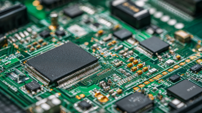
Key Components and Materials Used in PCB Fabrication
Understanding the key components and materials used in printed circuit board (PCB) fabrication is crucial for anyone involved in electronics design. A PCB typically consists of several key layers: the substrate, insulating materials, and conductive paths, often made from copper. According to a report by IPC, the global PCB market reached approximately $61 billion in 2021 and is projected to grow annually by 5.7% through 2026, highlighting the increasing demand for sophisticated PCB designs in various applications, from consumer electronics to advanced automotive systems.
When selecting materials for PCB fabrication, it’s essential to prioritize quality and performance. For instance, FR-4 is the most commonly used material for the substrate, providing excellent mechanical and thermal properties. Additionally, materials like polyimide are becoming more prevalent in flexible PCB applications due to their superior thermal stability. Tip: Always consider the thermal management properties of your PCB materials, as this can greatly influence the reliability and longevity of electronic devices.
Moreover, components like resistors, capacitors, and integrated circuits are integral to PCB functionality. The type and arrangement of these components can significantly affect circuit performance. Tip: Optimize the layout by placing high-frequency components close together to minimize signal loss and enhance electrical performance. Investing time in understanding the intricate details of PCB components and materials can lead to more efficient designs and improved product outcomes.
Top Tips for Understanding Printed Circuit Board Design and Applications - Key Components and Materials Used in PCB Fabrication
| Component |
Material |
Function |
Application Areas |
| Resistor |
Carbon Film |
Limits Current Flow |
Signal Processing, Power Regulation |
| Capacitor |
Ceramic |
Stores Electric Charge |
Timing Applications, Filtering |
| Inductor |
Ferrite Core |
Stores Magnetic Energy |
Power Supply Circuits, RF Applications |
| Microcontroller |
Silicon |
Performs Computation and Control |
Consumer Electronics, Robotics |
| PCB Substrate |
FR-4 |
Base Material for Circuit Layers |
General PCB Fabrication |
| LED |
Gallium Nitride |
Light Emission |
Lighting, Display Technology |
Common PCB Design Techniques and Best Practices
When it comes to printed circuit board (PCB) design, understanding common techniques and best practices is crucial for achieving optimal functionality and reliability. One of the fundamental techniques is the use of a careful layout process. According to a report by IPC, approximately 30% of PCB failures are attributed to poor design practices. To mitigate this, designers must focus on creating a balanced arrangement of components, ensuring that high-speed signals are routed in a way that minimizes interference. Techniques such as differential pair routing and controlled impedance can significantly enhance performance in RF and high-speed digital applications.
Another important best practice is the implementation of design rule checks (DRC) throughout the design process. By utilizing automated tools that identify potential issues related to spacing, trace width, and layer stacking, designers can avoid common pitfalls that may lead to functional failures. A survey conducted by EDN showed that PCBs designed with DRC in place experience a 25% decrease in time-to-market, highlighting the efficiency gained through diligent adherence to design rules. Incorporating simulation tools early in the design phase can also save time and resources by allowing engineers to predict and analyze circuit behavior before physical prototypes are created, further solidifying the importance of proper techniques and methodologies in PCB design.
Common PCB Design Techniques and Their Importance
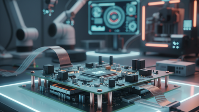
Applications of PCBs in Various Industries
Printed Circuit Boards (PCBs) are integral to a wide array of industries, serving as the backbone of electronic devices. In the consumer electronics sector, PCBs are found in everything from smartphones to laptops. Their role is crucial as they facilitate the interconnection of various components, enabling devices to function efficiently. The compact design of PCBs also allows for more miniature devices without compromising performance, which is essential in a market driven by innovation and portability.
Beyond consumer electronics, PCBs play a significant role in automotive applications. Modern vehicles rely heavily on electronic systems for functions like navigation, safety features, and engine management. PCBs enable the effective integration of sensors and control units, improving operational efficiency and enhancing safety. Moreover, in the medical field, PCBs are essential in devices such as imaging systems and monitoring equipment, where precision and reliability are paramount to patient care. The versatility of PCB design allows for customization that meets the stringent requirements of these high-tech industries, ensuring that they can support advancing technologies well into the future.
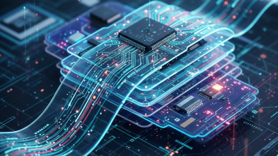
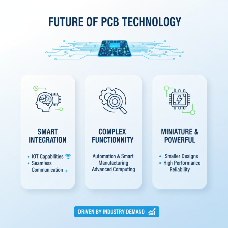
Future Trends in PCB Technology and Development
The future of Printed Circuit Board (PCB) technology is poised for significant advancements driven by the growing demands of various industries. One of the most notable trends is the increased integration of smart technologies into PCB design. This includes the incorporation of IoT (Internet of Things) capabilities, enabling devices to communicate and interact seamlessly. As industries shift toward automation and smart manufacturing, PCBs will evolve to support more complex functionalities, allowing for miniature designs while maintaining high performance and reliability.
Additionally, sustainability in PCB development is becoming increasingly crucial. The industry is moving towards the use of eco-friendly materials and processes to minimize environmental impact. Recycling and the reuse of materials are gaining traction, with manufacturers exploring biodegradable substrates and lead-free soldering techniques. This commitment to sustainability not only addresses environmental concerns but also responds to consumer demand for greener products. As technology continues to evolve, PCBs will play a pivotal role in shaping the next generation of electronic devices while adhering to environmentally responsible practices.