What Is an Electronic PCB Board?

What Is an Electronic PCB Board?

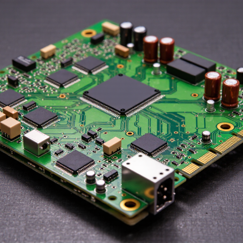
An electronic pcb board, more precisely called a printed circuit board (PCB), is the physical foundation of many modern electronic products. It connects and supports components such as integrated circuits, resistors, capacitors, connectors, and sensors. Instead of using separate wires, a PCB uses copper traces to carry electrical signals across a structured surface. Vias connect different copper layers, while solder masks protect exposed tracks from contamination and accidental shorts. The familiar green color is only a surface finish, not the board’s essential function.

It is everywhere.

A typical multilayer board may contain fiberglass-reinforced laminate, copper foils, plated holes, and carefully controlled impedance paths. These details influence heat dissipation, signal integrity, reliability, and manufacturing cost. IPC standards, including IPC-2221 and IPC-A-600, provide widely recognized guidance for PCB design and acceptance criteria. They help engineers evaluate spacing, materials, workmanship, and fabrication quality.

The market also reflects the board’s growing importance. Fortune Business Insights estimated the global PCB market at approximately USD 89.7 billion in 2023, with continued expansion expected through the next decade. Grand View Research has reported a comparable long-term growth direction, although market values vary by product categories and research methods. That difference deserves attention. Market forecasts are useful, but they are not guarantees.

From smartphones and vehicle control units to medical instruments and industrial robots, the electronic pcb board quietly determines how reliably a device performs. Understanding its layers, materials, and manufacturing process makes product specifications easier to judge. It also reveals an uncomfortable truth: a small design oversight can create expensive failures later.
What Is an Electronic PCB Board?

Definition and Basic Purpose of an Electronic PCB Board

What Is an Electronic PCB Board?

An electronic PCB board, or printed circuit board, is the physical platform inside many electronic products. Its basic purpose is simple: it connects components and directs electrical signals. Copper traces act like controlled pathways across a flat insulating material. Soldered components, such as resistors, capacitors, and integrated circuits, perform specific electrical tasks. The board also provides mechanical support, so parts stay aligned during use, testing, and repair.

A PCB is more than a plate with metal lines. Its layers manage power, signals, heat, and physical strength. A single-layer board may suit a simple sensor. Complex equipment often needs multiple copper layers and carefully controlled impedance. Grand View Research estimated the global PCB market at approximately 89.7 billion US dollars in 2023. Its 2024 analysis also projected continued growth through 2030. This expansion reflects rising demand for compact electronics, although market estimates can change with material costs and production conditions. That uncertainty deserves attention.

Tips: Check the board’s layer count, copper thickness, hole quality, and operating temperature. These details often reveal more than appearance. Keep signal paths short where possible. A neat layout is not automatically a reliable one. Designers should review clearances, grounding, and heat dissipation before production. In practice, even experienced teams can miss a small spacing problem. Careful testing remains necessary.

Main Components and Layers of a PCB

What Is an Electronic PCB Board?

Main Components and Layers of a PCB

An electronic PCB board is a rigid or flexible platform that connects electrical components. It replaces much of the point-to-point wiring found in older equipment. Copper traces carry current and signals across the board. Their width, spacing, and length affect heat, resistance, and signal quality.

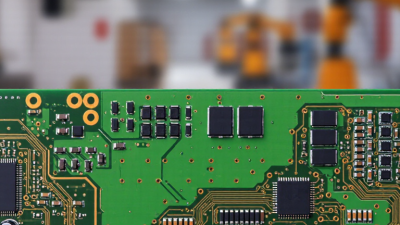
A typical PCB contains several functional layers. The substrate provides mechanical support and electrical insulation. In multilayer designs, copper signal layers carry data and power. Ground and power planes help control noise and distribute energy evenly. Prepreg bonds the layers together, while vias create conductive paths between them. The solder mask covers exposed copper and helps prevent accidental bridges. Silkscreen markings identify component locations and test points.

Small details matter.

Common components include resistors, capacitors, diodes, integrated circuits, connectors, and oscillators. Each part has a defined position and purpose. Pads provide soldering surfaces, while mounting holes secure the board or connect it to a chassis. During inspection, technicians check solder joints, polarity marks, trace damage, and unwanted copper connections. Heat can reveal weak layouts, especially near power components. Moisture and contamination can also reduce insulation performance over time. A design may look correct on a screen yet fail during vibration or thermal testing. That gap deserves honest review. Good PCB work depends on calculated spacing, verified materials, controlled assembly, and testing under realistic conditions.

How an Electronic PCB Board Works

What Is an Electronic PCB Board?

An electronic PCB board is a flat platform that connects components through copper pathways. It carries power and signals between resistors, processors, sensors, and connectors. The board usually contains insulating layers, copper traces, drilled holes, and protective solder masks. These details look simple. They are not.

How an Electronic PCB Board Works

Electric current enters through a connector or power section. Copper traces then guide it across the board, much like narrow roads guiding traffic. Components change, control, or measure that current. A resistor limits flow, while a capacitor stores energy briefly. A processor interprets signals and sends new instructions through other traces.

Layer arrangement matters. Power planes reduce voltage loss, and ground planes help control electrical noise. Designers also calculate trace width, heat buildup, and signal timing. IPC-2221 provides widely used design guidance for these decisions. In practice, tiny errors can create weak solder joints or unexpected interference.

The market is expanding. Grand View Research estimated the global PCB market at about 89.7 billion U.S. dollars in 2023 and projected continued growth through 2030. More boards also create more responsibility. The Global E-waste Monitor 2024 reported 62 million tonnes of electronic waste in 2022. Repairable layouts and reliable materials can extend product life. Yet no layout is perfect. I still see designers prioritize compactness over serviceability, and that choice deserves more reflection.

What Is an Electronic PCB Board? - How an Electronic PCB Board Works

Data Dimension Typical Information How It Relates to PCB Operation
Basic Definition Printed Circuit Board (PCB) A rigid or flexible board that mechanically supports electronic components and electrically connects them through conductive copper patterns.
Main Structural Layers Substrate Copper Solder Mask Silkscreen The substrate provides mechanical support, copper carries electrical signals, the solder mask protects exposed copper, and the silkscreen provides identification markings.
Common Substrate Glass-reinforced epoxy laminate, commonly classified as FR-4 The insulating substrate separates conductive layers and helps maintain the board’s mechanical strength and electrical isolation.
Conductive Material Electrolytic or rolled copper Copper forms traces, pads, planes, and plated holes that carry current or electrical signals between components and circuit layers.
Typical Board Types Single-sided, double-sided, multilayer, rigid, flexible, and rigid-flex The selected construction determines routing capacity, mechanical flexibility, manufacturing complexity, and suitable application environments.
Typical Layer Count 1 to more than 20 conductive layers, depending on circuit complexity Additional layers provide more routing space and dedicated power or ground planes while increasing thickness and manufacturing requirements.
Circuit Connections Traces, pads, vias, and plated through-holes Traces connect circuit nodes, pads provide component connection areas, and vias connect copper patterns between different board layers.
Component Mounting Methods Through-hole technology and surface-mount technology Through-hole leads pass through drilled holes, while surface-mount components are attached directly to pads on the board surface.
Power Distribution Power traces, copper pours, and dedicated power or ground planes These structures distribute supply voltage and return current while helping reduce voltage drop and unwanted electrical interference.
Signal Path Source component → copper trace → vias or layers → destination component An electrical signal travels through a designed conductive path, with the trace geometry and surrounding materials affecting its resistance and signal behavior.
Electrical Insulation Nonconductive dielectric material between copper layers Dielectric layers prevent unintended current flow between adjacent conductive layers and influence capacitance and controlled-impedance routing.
Thermal Management Copper areas, thermal vias, heat sinks, and board airflow Heat generated by components can be spread through copper and transferred away from hot areas to improve reliability and operating stability.
Protection Features Solder mask, conformal coatings, fuses, and protective circuit sections These features help protect conductors and components from solder bridges, moisture, contamination, overcurrent, or other operating hazards.
Manufacturing Sequence Design layout → imaging or pattern formation → etching or plating → drilling → lamination → solder mask → assembly → testing Each stage creates or verifies the conductive paths, insulation, mechanical structure, and component connections required for the finished circuit.
Design File Information Board outline, copper layers, drill data, component locations, solder-mask openings, and assembly data These digital definitions communicate the physical dimensions, electrical connections, and manufacturing requirements of the PCB.
Testing Methods Visual inspection, electrical continuity testing, insulation testing, and functional testing Testing checks for manufacturing defects such as open circuits, short circuits, incorrect assembly, and failure to perform the intended circuit function.
Key Reliability Factors Temperature, humidity, mechanical stress, current density, solder quality, and material selection These factors influence service life, dimensional stability, connection integrity, and the PCB’s ability to operate consistently.
Primary Function Mechanical support, electrical interconnection, signal routing, and power distribution A PCB integrates these functions into a compact platform so an electronic circuit can be assembled, powered, controlled, and tested as a complete system.

Common PCB Types and Their Applications

What Is an Electronic PCB Board?

Common PCB Types and Their Applications

An electronic PCB board connects components through copper traces on an insulating base. It carries signals, distributes power, and supports mechanical assembly. The board type affects durability, cost, heat control, and repair access. In practical design reviews, engineers check the operating environment before choosing materials.

Rigid PCBs are common in computers, control panels, instruments, and household equipment. They keep their shape and support stable component placement. Flexible PCBs bend inside cameras, wearable devices, and compact medical equipment. They reduce wiring space, but repeated bending can damage traces. Rigid-flex boards combine both structures for aerospace controls, robotic joints, and small industrial modules. Fit matters.

Single-sided boards work well in simple circuits, sensors, and low-cost controls. Double-sided boards provide more routing space for power supplies and measurement devices. Multilayer PCBs handle dense processors, communication equipment, and complex automation systems. Metal-core boards move heat away from high-power LEDs and converters. High-frequency boards require carefully controlled materials and trace geometry.

The boundary is not always clean. A flexible board may solve space problems but complicate assembly and inspection. A multilayer design can improve performance while increasing manufacturing risk. Engineers should review temperature, vibration, moisture, current load, and service conditions together. A cheaper board can become expensive after field failures. Careful testing still matters.

PCB Manufacturing, Assembly, and Quality Testing

What Is an Electronic PCB Board?
PCB Manufacturing, Assembly, and Quality Testing

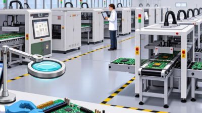
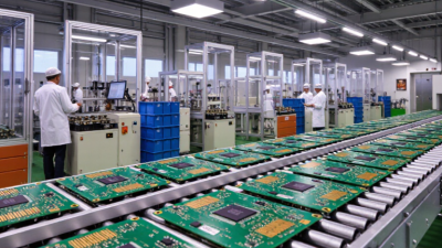
An electronic PCB board is a rigid or flexible platform that connects electronic components. Copper traces carry signals and power across carefully designed layers. During manufacturing, engineers convert digital layouts into physical circuit boards. The process usually includes imaging, etching, drilling, plating, solder-mask coating, and surface finishing. Small errors matter. A blocked hole or uneven copper layer can affect the entire assembly.

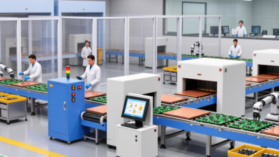
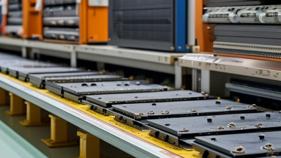
PCB assembly begins after the bare board passes initial inspection. Automated equipment places resistors, capacitors, integrated circuits, and connectors with precise alignment. Solder paste forms controlled joints during reflow heating. Technicians may add larger components by hand when shape or placement requires extra care. Assemblers inspect solder volume, component orientation, and board cleanliness. Production records should identify materials, operators, equipment settings, and inspection results.

Quality testing combines visual checks with measurable electrical evidence. Automated optical inspection can detect missing parts, shifted components, and solder bridges. Flying-probe or fixture-based tests verify continuity and isolation. Functional testing then applies controlled power and checks real operating behavior. Test limits must be documented, not guessed. Even experienced teams can overlook a weak connection hidden beneath a component. Reviewing failure patterns helps improve stencil design, thermal profiles, and operator training. A perfect first-pass rate may look impressive, but honest data is more useful when it reveals recurring defects.

Search our website