Why Is Electronics PCB Manufacturing Important?
A smartphone wakes with one tap. A medical monitor tracks a heartbeat. Behind both is a printed circuit board, connecting components through carefully formed copper paths. Electronics pcb manufacturing turns circuit designs into physical systems that can be assembled, tested, and used reliably. Small defects matter: a weak solder pad or poorly controlled trace can interrupt a signal or shorten a product’s life.
The scale is significant. The World Semiconductor Trade Statistics organization reported worldwide semiconductor sales of $627.6 billion in 2024, a 19.1% increase from 2023. Semiconductors need boards to connect them to power, sensors, displays, and other components. That makes PCB production a practical foundation for a much larger electronics supply chain. It also means manufacturers must control materials, drilling, imaging, plating, and inspection with care.
Signal integrity expert Eric Bogatin, author of Signal and Power Integrity—Simplified, often teaches: “A signal is not a voltage. A signal is a change in voltage.” The idea helps explain why trace geometry and board construction affect real product performance. A board is not merely a flat holder for parts. It shapes how signals and power move.
The industry’s growth, though, is not the whole story. Faster production can still create waste or rework when process control slips. Good manufacturing depends on repeatable methods, skilled inspection, and honest testing. That is less glamorous than a new device. It is essential all the same.
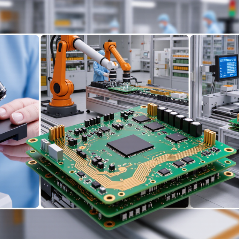
Electronics PCB manufacturing turns circuit design files into a physical board that carries signals and power. The process begins with files defining copper paths, hole locations, layer order, and board dimensions. Fabricators check spacing, drill sizes, and material choices before production. A board may have one copper layer or several bonded layers, depending on its electrical and routing needs. Copper foil is laminated to a base material, and imaging transfers the circuit pattern. Etching then removes unwanted copper. Small details matter. A misplaced hole or overly narrow trace can create problems during assembly.
Next, manufacturers drill the board and plate holes with copper to connect layers. They apply a solder mask to protect exposed copper, then print labels that identify components and connections. Multilayer boards require careful alignment and pressure during bonding; even slight shifts can affect internal connections. Automated optical inspection checks visible features, while electrical tests look for opens and shorts. Some defects are hard to spot, so a clean image alone is not proof of a reliable board. Test coverage and clear production records matter. The process is precise, but it is not infallible; reviewing design assumptions before fabrication can prevent avoidable rework.
| Manufacturing Stage | What It Involves | Why It Matters | Typical Output or Check |
|---|---|---|---|
| Design preparation | Reviewing circuit-board layout files, layer information, hole locations, and manufacturing requirements before production. | Early checks can identify layout or documentation issues that could affect manufacturability, cost, or reliability. | Manufacturing-ready design data and documented production requirements. |
| Substrate and copper preparation | Selecting the board material and preparing copper-clad laminate for the required layer structure. | The substrate and copper stack influence electrical insulation, mechanical support, heat behavior, and board thickness. | Prepared laminate with the specified material and layer arrangement. |
| Circuit pattern formation | Transferring the circuit pattern to copper and removing unwanted copper through etching. | Accurate copper traces and clearances help establish electrical connections while reducing the risk of shorts or open circuits. | Patterned copper layers inspected for line features and defects. |
| Drilling and via formation | Creating holes for component leads and vias; plated-through holes receive conductive copper plating where required. | Vias and plated holes connect circuit layers, while component holes support through-hole assembly. | Hole locations and sizes checked against the board design. |
| Layer alignment and lamination | Aligning inner and outer layers and bonding multilayer boards under heat and pressure. | Accurate registration and bonding are important for electrical connectivity and the board’s structural integrity. | Bonded multilayer panel checked for alignment and lamination quality. |
| Solder mask and legend | Applying solder mask over selected copper areas and printing component identifiers or other markings when specified. | Solder mask helps protect copper and reduce unintended solder bridging; markings support assembly and service. | Coverage, openings, and printed details checked against the design. |
| Surface finish | Applying a suitable finish to exposed copper pads to protect them and support soldering. | The finish affects pad protection, solderability, and compatibility with the intended assembly process. | Finished pads inspected for coverage and surface condition. |
| Board profiling and inspection | Separating boards from production panels and checking dimensions, edges, and visible features. | Correct board outline and dimensions help ensure the PCB fits its enclosure and assembly equipment. | Profile and dimensions verified against the drawing or design data. |
| Electrical testing | Testing specified connections for continuity and checking for unintended shorts between conductors. | Electrical tests help identify manufacturing defects before boards proceed to electronic assembly. | Test results recorded against the board’s electrical test requirements. |
| Assembly interface | Providing a finished bare PCB for component placement and soldering in a separate assembly process. | A well-manufactured board supports accurate component mounting and reliable electrical interconnection. | PCB supplied with documented specifications and inspection results as required. |