What Is the Best PCB Manufacturing Process in 2026?
Choosing the best pcb process in 2026 starts with the board’s purpose, not a factory’s sales claim. A compact, two-layer sensor board has different needs from a dense multilayer controller carrying high-speed signals. Board size, copper weight, line spacing, via design, expected quantity, and budget all affect the right manufacturing route. There is no universal winner. That is less satisfying, but more useful.
A dependable process connects engineering decisions with controlled production: design review, material selection, imaging, etching, drilling, copper plating, solder-mask application, surface finishing, and inspection. Each stage can influence yield and reliability. For example, a very small annular ring may save space, yet leave less tolerance for drilling variation. Ask suppliers to review the stack-up and fabrication notes before release, and confirm their capabilities against your actual tolerances. Request clear acceptance criteria and inspection records, such as electrical test results and dimensional checks. For prototypes, quick turnaround may matter most; for repeat production, consistency, traceability, and stable material sourcing often deserve greater weight. Still, process labels alone do not prove quality. Compare documented capabilities, sample reports, and communication, then reassess the choice when the design changes. A careful review can prevent expensive surprises, though no process removes every risk.

Defining the Best PCB Manufacturing Process for 2026
Defining the Best PCB Manufacturing Process for 2026
The best PCB manufacturing process is the one that meets a board’s electrical, mechanical, and production needs—not simply the one with the smallest quoted price. Prismark’s 2024 industry review put global PCB production value at roughly US$73 billion, reflecting a large market with varied product demands. That scale does not make every process suitable for every design. A compact, high-speed board may need fine traces, controlled impedance, and careful layer registration. A simple control board may benefit more from standard materials and a less complex stack-up. The choice depends on measurable requirements: operating frequency, layer count, copper weight, expected volume, and acceptable defect rates.
Tips: Ask manufacturers to review the stack-up, minimum trace and spacing, and drill sizes before finalizing the layout. Request panelization and inspection details, too. IPC-6012 provides qualification and performance requirements for rigid printed boards; use the applicable class and acceptance criteria when comparing supplier proposals. Then compare yield, lead time, and total cost—not unit price alone. A process that works in a prototype run may behave differently at production volume. That gap deserves attention. Even experienced teams can underestimate it.
What Is the Best PCB Manufacturing Process in 2026?
Defining the best process starts with the board’s electrical, thermal, and mechanical requirements.
Standard copper weights correspond to different nominal foil thicknesses: 0.5 oz/ft² is about 17.1 µm, 1 oz/ft² about 34.3 µm, 2 oz/ft² about 68.6 µm, and 3 oz/ft² about 102.9 µm. Thicker copper can support higher current, but may affect trace spacing and fabrication requirements. The best PCB process is the one that meets the application’s needs—not simply the one with the thickest copper.
Selecting Materials, Layer Counts, and Production Methods
Choosing a PCB process in 2026 starts with the board’s job, not a fashionable material. Standard FR-4 suits many control boards and everyday electronics. For high-speed signals, compare dielectric constant and loss, not just the laminate’s price. A long trace can behave differently when material properties vary. Check operating temperature, copper weight, and board thickness against the actual design.
Keep the layer count as low as the routing allows. Two layers can work for simple circuits, while dense designs may need four or more for routing space and stable reference planes. More layers add pressing, drilling, and inspection steps. They also increase cost. But squeezing a crowded design onto fewer layers can create awkward routing and signal problems. There is no perfect stack-up.
Production method matters, too. A small prototype run can reveal whether connectors fit and fine-pitch parts assemble cleanly. For repeat production, consistent materials, panel utilization, hole sizes, and documented tolerances become more important. Ask the fabricator to review the stack-up and minimum features before release. A 0.2 mm drill may seem like a small detail; it can affect yield. I would still question any design that chooses a process by price alone. The cheaper quote is not always the cheaper board.
Preparing PCB Designs for Fabrication
The best PCB manufacturing process in 2026 starts before the board reaches a production line. A clean design gives the fabricator clear geometry, realistic tolerances, and a stackup suited to the board’s intended use. Small decisions matter. Set copper weights, dielectric thicknesses, and finished board thickness together, rather than treating them as separate choices.
Check every footprint against the component datasheet, especially pad pitch and hole size. Compare trace and spacing rules with the fabricator’s capabilities; tighter is not automatically better. A 0.15 mm clearance may look neat in CAD, but it can raise costs or lower yield. Review annular rings, solder-mask openings, and copper-to-edge distance. Check them twice.
Before release, run electrical and design-rule checks, inspect the board in 3D, and verify the fabrication notes. Export the required copper, mask, drill, and outline data, then confirm that all files describe the same revision. A short manufacturing review can catch mirrored layers or missing slots before panels are made. Even careful checks miss things; a quote may expose assumptions the drawing did not make clear. Unusual materials or dense layouts may need direct engineering discussion, so leave room for that conversation.
Fabricating and Assembling the Circuit Board
The best PCB manufacturing process in 2026 starts with a design that can be built consistently. Before fabrication, engineers review the stackup, copper thickness, trace spacing, and drill sizes against the board’s electrical and mechanical needs. A small change in via placement can prevent a crowded assembly area later. Details matter.
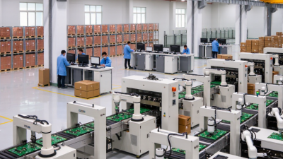
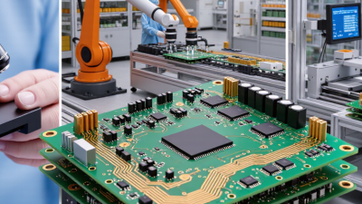
Fabrication typically moves from copper-clad laminate through imaging, etching, drilling, plating, and solder-mask application. Each stage needs measurable checks: confirm finished hole sizes, inspect copper features, and verify that the board outline matches the drawing. Then comes assembly. Solder paste is applied through a stencil, components are placed on the pads, and controlled reflow heat forms the joints. Automated optical inspection can catch shifted parts or uneven solder, while selected boards may need electrical testing.
Good process choices depend on volume, board complexity, component pitch, and reliability needs—not on one universal recipe. A prototype may benefit from quick-turn fabrication, while a dense production board needs tighter control of materials and process variation. I would not treat inspection as a cure for weak design reviews; it finds defects, but it cannot make every layout easy to build. A practical handoff includes clear fabrication notes, assembly drawings, and defined test requirements. Even then, first builds can reveal awkward access for probes or components that crowd a connector. Those findings should feed into the next revision.
Evaluating Quality, Reliability, Cost, and Sustainability
What Is the Best PCB Manufacturing Process in 2026?
Evaluating Quality, Reliability, Cost, and Sustainability
The best PCB process depends on the board’s actual demands, not the newest equipment. A fine-pitch design may need tighter layer registration and laser-drilled microvias. A simpler control board may work reliably with standard drilling and fewer layers. Ask manufacturers how they verify copper thickness, hole quality, and trace spacing. Inspection records matter more than a polished capability chart. Small defects can become costly failures after repeated heating or vibration.
Reliability starts with matching materials to the operating environment. Check temperature ratings, laminate moisture behavior, and test-coupon results. For production, compare electrical testing coverage and the process used to track defects.
Cost includes more than the quoted price. Extra layers, tight tolerances, and low-volume setups can raise tooling and inspection costs. Sustainability deserves specific questions: What happens to copper-bearing waste? Are water and energy use measured per production run? Vague claims are hard to evaluate.
One uncomfortable trade-off remains: a highly optimized design may reduce material use but leave less margin for manufacturing variation. Engineers should review yield data and failure reports, then revisit assumptions before approving a process.